
Accelerate

Device Development

and 3D Advanced Packaging

with Process-Driven Simulation

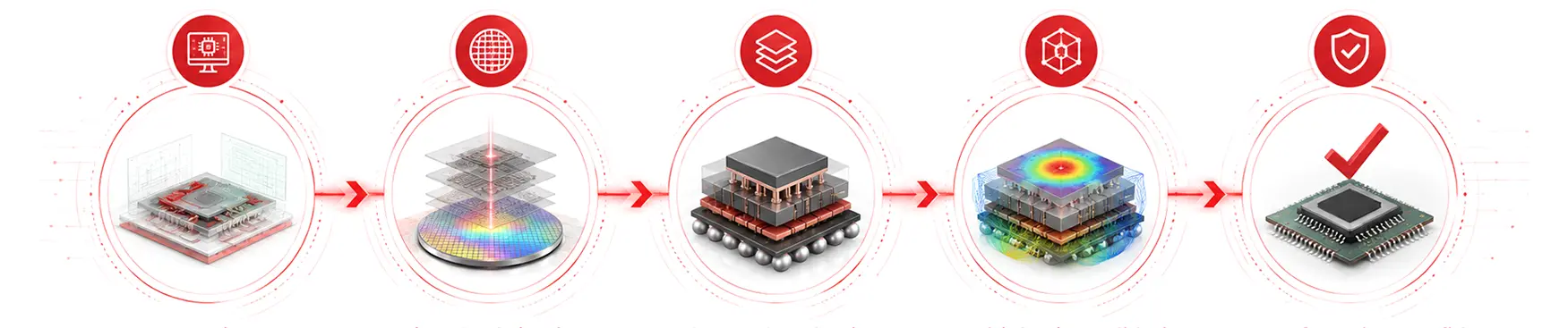
Virtual Fabrication arrow Multi-Physics arrow Performance

Develop Advanced Semiconductor Devices with IntelliSuite®.

Simulate Microfabrication Process, Optimize device recipe,

3D Advanced Packaging, Multiphysics, MEMS and EDA linker.

A complete workflow from concept until Manufacturing.

email whatsapp call
cards

100+

MICROFABRICATION PROCESS MODULES

cards

3D

ADVANCED PACKAGING

cards

FAST-FIELD

MULTIPHYSICS ANALYSIS

cards

UPTO

50%

SHORTER DEVICE DEVELOPMENT CYCLE

cards

PROCESS-TO-PERFORMANCE

WORKFLOW

TRUSTED BY FAB & FABLESS COMPANIESRESEARCH LABSUNIVERSITIESTECHNOLOGY LEADERS

RE Research University of Windsor Cornell University Kyoto University OE Solutions
semicon logo

Experience IntelliSuite® LIVE at SEMICON India 2026

See the complete Process-to-Performance workflow demonstrated by our technical experts. Discuss your engineering challenges and discover how process-driven simulation, combined with fast-field multiphysics iterations, improves device performance, accelerates innovation, and can reduce device development cycles by up to 50%.

SEPTEMBER 17 - 19, 2026|HALL NO. 02|BOOTH NO. H7729|YASHOBHOOMI, DELHI, INDIA

IntelliSuite®

One Unified Platform for Semiconductor Innovation

Accelerate Semiconductor innovation through process simulation for device recipe optimization and 3D advanced packaging. Predict realistic behavior of devices before and after packaging through our Multiphysics simulation approach on process driven models. Further, link it to EDA tools through EDA linker. Thus making it a complete simulation solution platform from virtual fabrication arrow Multiphysics arrow EDA arrow build solutions towards gaining manufacturing confidence.
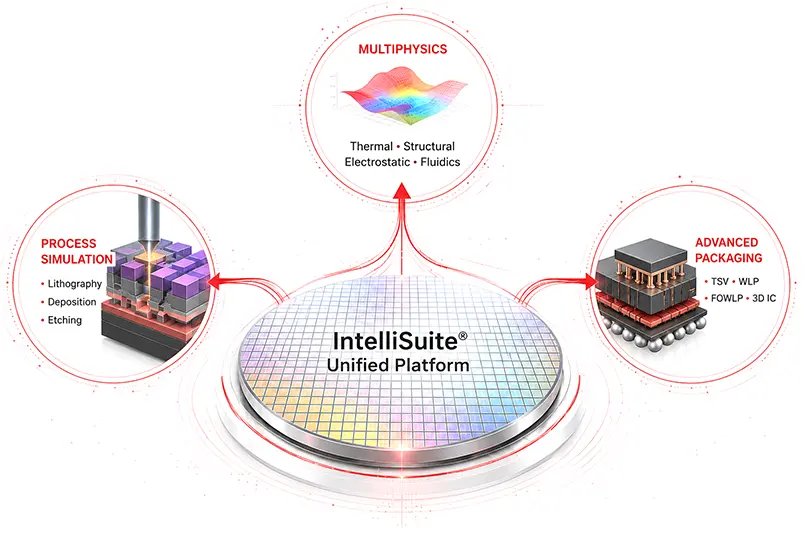
IntelliSuite® enables engineers to model, simulate, validate, and optimize semiconductor devices within one unified environment. By combining realistic fabrication process simulation with advanced packaging and multiphysics analysis, teams can predict device performance before manufacturing—reducing design iterations, lowering development costs, and accelerating time to market.

isuite
workflow-img

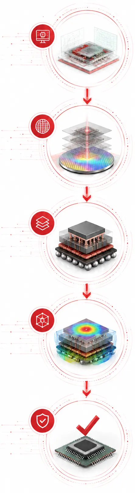
Design

Conceptualize and model your device with precision.

Virtual Fabrication

Simulate real-world fabrication processes to build accurate virtual models.

Advanced Packaging

Design and validate next-generation packaging technologies including TSV, WLP, FOWLP, 3D IC and more.

Multiphysics Validation

Analyze thermal, structural, electrostatic, fluidic and coupled physics to ensure optimal performance and reliability.

Manufacturing Confidence

Gain confidence with verified designs and accelerate time-to-market with reduced risk.
workflow-img

Design

Conceptualize and model your device with precision.

Virtual Fabrication

Simulate real-world fabrication processes to build accurate virtual models.

Advanced Packaging

Design and validate next-generation packaging technologies including TSV, WLP, FOWLP, 3D IC and more.

Multiphysics Validation

Analyze thermal, structural, electrostatic, fluidic and coupled physics to ensure optimal performance and reliability.

Manufacturing Confidence

Gain confidence with verified designs and accelerate time-to-market with reduced risk.

IntelliSense®
Trusted by Semiconductor Innovators and Experts Worldwide

Discover how semiconductor companies, research institutions, and technology innovators leverage IntelliSuite® to accelerate development, optimize fabrication workflows, and bring breakthrough products to market with greater confidence.

picture
quote

This feature is a critical new addition for our products development and optimisation. We are pleased with the capabilities it brings to exploring various processing options. While working with IntelliSense team, they have addressed our requirements seriously and result of the development is this great new feature


OE Solutions America Inc

picture
quote

“Polaris,” developed by #GeneralElectric (GE) scientists, is a foundry process flow for developing high precision navigation grade MEMS devices. This MEMS process enables high-precision navigation devices without GPS. Todd Miller is excited about partnering with IntelliSense Software and says, by modeling “Polaris” in IntelliSuite and providing a process development kit (PDK), will enable customers into GE's fab faster with fewer costly mistakes. Sripadaraja K worked closely with the GE Polaris development team to bring this on IntelliSense Software.


GE Research

Thank You!

Our team has received your request.