


Welcome to IntelliSense: Leading the Way in Process Modeling Solutions
At IntelliSense, we specialize in providing state-of-the-art process modeling solutions tailored to meet the unique needs of our clients.
Welcome to our platform, where innovation meets efficiency in process modeling.
Our process modeling software sets the industry standard, offering a comprehensive suite of tools designed to streamline every aspect of the modeling process. From conceptualization to analysis, our intuitive platform empowers engineers to develop precise and efficient process models with ease.
With IntelliSense process modeling software, you gain access to advanced simulation capabilities that enable you to predict and optimize the performance of your processes. Our robust algorithms allow for in-depth analysis of various parameters, ensuring optimal efficiency and productivity in real-world applications.
Ready to optimize your processes and drive efficiency? Explore the possibilities with IntelliSense and experience the future of process modeling today.
AnisE is an easy-to-use anisotropic etch process simulation tool for MEMS design and process control
Anisotropic etching is one of the most difficult silicon micro-machining processes to model, often considered in the realm of the black arts. It can be challenging to grasp intuitively due to the complex nature of evolving etch fronts. In fact, many companies have developed closely guarded etch secrets through trial-and-error experimentation.
Well, those days have ended. AnisE simplifies the process of accurately simulating etch behavior. Import your mask, choose your wafer orientation and your process parameters, and then watch the etching progress online before your eyes!
Unlike other tools that utilize heuristic methods to calculate propagation of etch planes, AnisE is a cellular automata based simulation. What does this mean? That other tools fail to provide accurate results for complex masks and long etch times. With AnisE, you can choose any mask configuration, however complex, throw in double-sided etching and add etch stops. Its easy
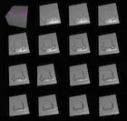
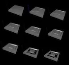

3D evolution of Silicon etch profiles generated by AnisE are shown in three cases. (a) evolution of three different corner compensation schemes (b) double-sided etching of a silicon boss for an accelerometer application and (c) multi-etch of silicon, an example where DRIE is followed by an anisotropic etch.
AnisE comes with built-in etch databases for KOH and TMAH. It automatically updates the etch rates as a function of temperature and concentration.
With AnisE, you can simulate single or double-sided <100> and <110> etching. You can incorporate multiple etch stops, steps or anything else you can do in the real world. In addition, you can study the effect of mask misalignment, the effect of combining RIE etching with anisotropic etching and many other real- world conditions.
Whether you are interested in studying process variation or designing corner compensation features, AnisE will become an invaluable part of your process toolset.
AnisE is capable of predicting the effects of etchant temperature, concentration, and etch time on the final 3D device geometry. Corner compensation and process tolerances can be modeled and visualized with AnisE. Creating correct geometries based on proper etch parameters before entering a fabrication facility saves resources otherwise spent on multiple prototype iterations.


By creating or importing a mask file, users can:
 Simulate <100> or <110> wafer orientation etching
 Simulate etching under different time, temperature, and concentration parameters
 Access TMAH and KOH etch-rate databases, or use customized etch-rate data
 Etch the top, bottom, or both sides of a wafer
 Implement multiple protective etch stops
 Perform multiple etchings with different masks on a single wafer
 Study the effects of misalignments and other process deviations
 Determine the effects of vertical etching coupled with anisotropic etching
 Perform 3D geometric visualization and cross-sectioning
 Take distance measurements on the etched wafer
 Visualize and export 3D results in DXF and VRML formats
IntelliEtch is an advanced ab initio based anisotropic etch process simulation tool for MEMS design and process control
Atomistic etch simulation IntelliEtch is a self-contained, user-friendly, multiscale atomistic simulator of wet and DRIE etching with multi-mask patterning capabilities. Based on an octree representation of the silicon sample, it uses both Kinetic Monte Carlo (KMC) and Cellular Automata (CA) algorithms for propagating the surface forward in time. In addition to offering assistance for MEMS engineering design, IntelliEtch enables a deeper insight of key features such as the atomistic structure of any surface orientation, the step flow nature of wet etching, and the development of characteristic morphologies in the evolving etch front.
With IntelliEtch, one can pattern and etch any surface orientation (not only the traditional {100}, {110} and {111} wafers), expanding the possibilities of MEMS design and enabling the testing of vicinal surface effects. Furthermore, IntelliEtch makes possible the patterning and etching of non-flat substrates with flat, round, vertical, or diagonal features. Even spherical silicon samples can be patterned and etched. It is also possible to explore and fine-tune a particular process by etching a structure atom-by-atom.
Using advanced ab initio (first principles) based simulation techniques, IntelliEtch can simulate down to atomistic scales. Whatever your etch scale, IntelliEtch handles it with panache
The simulator conveniently records modifications to each project as a separate file for easy reproduction and documentation, freeing the user from tedious bookkeeping tasks. The simulation state can be automatically saved at user-defined checkpoints, enabling the user to perform other tasks while running a simulation. After the simulation is complete, IntelliEtch offers easy integration with Finite Element Analysis software for thermal and mechanical analysis of the etched structure.
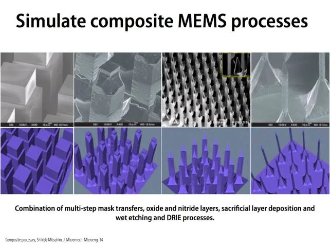
(a) Perform composite etches (b) Non-flat surfaces: simulate roughness and waviness effects
IntelliEtch can simulate complex MEMS structures by enabling:

First principle-based etch simulation; includes effects of steric interaction, backbond weakening, and impurity micromasking
Effects of multi-masking, multiple process steps

Predict high-order planes, surface morphology, and design corner compensations

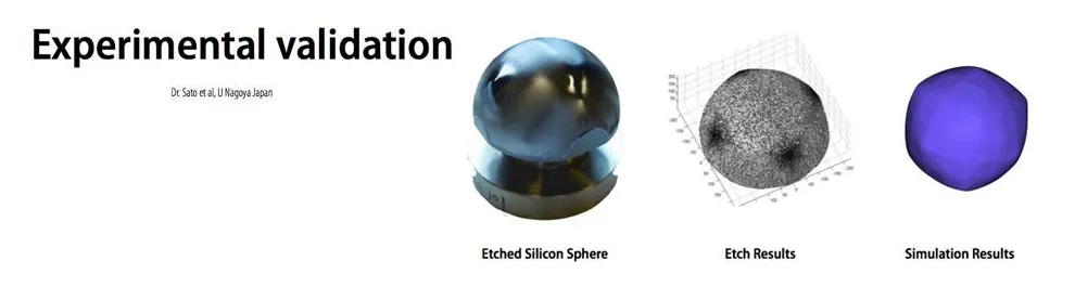
Detailed experimental backing

for etching based upon pioneering work of Dr. Sato at Nagoya University
Direct export to IntelliSuite and other industry formats
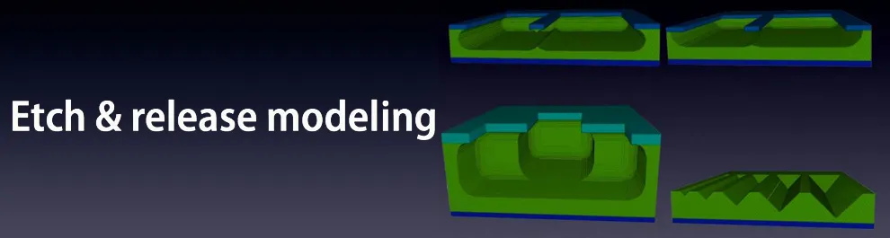
IntelliFAB allows you to debug your process flow and your mask set even before you enter the clean room. It allows you to make virtual prototypes to save costly fabrication mistakes.
Until now, MEMS designers have typically focused purely on geometric representation of the device in order to analyze device behavior. The drawback of this methodology is that process induced effects may vary the geometry of the structure significantly. For example, the boron diffusion as an etching stop layer for bulk silicon processing may overstress the structure, strain gradients in poly-silicon structures can distort features, or an anodic bonding process may break down protective oxide films.
IntelliFAB allows designers to takes a different approach. Process flow forms the basis of creating your devices. Our comprehensive process simulation modules incorporate deposition, etching, bonding, doping, electroplating, liftoff, and other process steps common in MEMS design. Other process-induced effects, such as micro-assembly, are also addressed to generate accurate geometric models for the complete range of MEMS devices. IntelliFAB is directly linked with MEMaterial, a MEMS process database that stores material properties as a function of your machine settings. By developing the fabrication process in conjunction with the analysis model, IntelliSuite enables engineers to perform more accurate device physics analysis and produce manufacturable devices faster.

A typical MEMS process flow can consist of hundreds of process steps which need to be cataloged and debugged; IntelliFAB makes editing and organizing large process tables easy. Built in grouping, filtering, and arrangement tools allow you to section, organize and debug large process tables.
IntelliFAB allows you to quickly build and debug your process traveler down to the last detail.
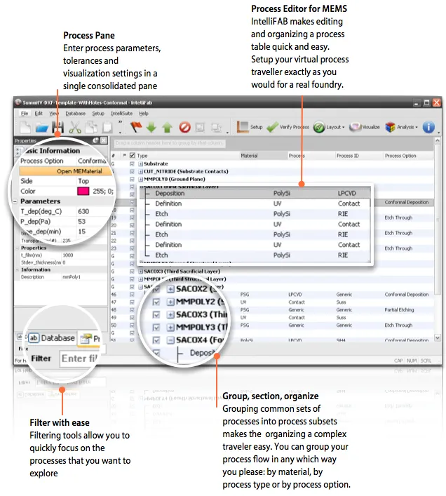
Processes can be custom-designed one step at a time, or engineers can draw from a wide range of foundry-ready process templates. Users create their own process flows from a database of over 70 process steps or by including custom process steps. Process flows can be saved as templates for repeated use.
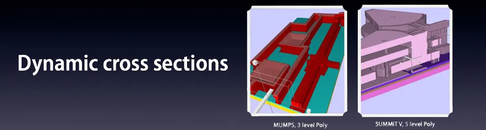
Support for popular processes MUMPS, SUMMiT-V, Infotonics (SOI Hybrid), AMI_MOSIS, Bosch Surface Micromachining, LIGA, Cornell SCREAM is included out of the box
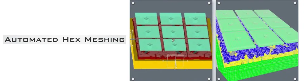
Hexpresso, our mesh synthesis tool is now integrated with IntelliFAB. With click of a button you can create high fidelity, all-hexahedral meshes from the process flow. MEMS Designers can spend up to 70% of their design person-hours creating and manipulating meshes. Solid models created by IntelliFAB can be directly exported to analysis engines with the click of a button, saving you considerable effort and time.
IntelliFAB uses true process information along with your mask layouts to create the device model for analysis.

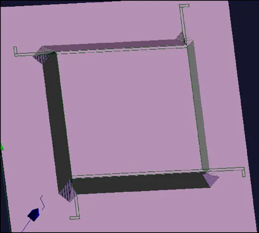
View FABViewer Cross-sectioning capability in real-time.
Virtual prototyping of a mechanism using the Summit-V process
See how FABViewer can help you in process debug

IntelliFAB Slideshow(Slideshare)

IntelliFAB Presentation PDF

As a packaging engineer, IntelliSense offers you tools for thermal, mechanical and high-frequency modeling of your devices. Parametric scripting capabilities allow you to effortlessly create a range of packages, such as SOICs, DIPs, QFPs etc. What's more, wafer-level encapsulation and related stress analyses may be performed with ease. As a result, you can wrap up your projects quickly and efficiently!

Working together, IntelliSuite and SYNPLE give test engineers a straightforward method for creating parametric test structures and design of experiments (DoE) during the layout process. What's more, our analysis and system simulation tools allow you to perform a vast subset of MIL-STD (750/883), JEDEC (JESD22) and Telcordia (Belcore) tests in software before the actual fabrication. For success in your next test, turn to IntelliSuite!
MEMaterial, the most comprehensive thin-film materials' knowledge base available today, provides a vital link between the process parameters and the device behavior. Use MEMaterial as an organization-wide database, knowledge repository, or as a tool to optimize processes in your fab.
As the most comprehensive thin-film materials' knowledge database and process optimization tool available today, MEMaterial provides a vital link between process parameters and device behavior. Introduced in 1993 and continuously updated, MEMaterial was the first software product to address the lack of thin-film material information. Linking actual fabrication machine settings to thin-film material properties marked a major milestone in the development of MEMS. By providing insight into the behavior of materials, MEMaterial helps eliminate the trial and error fabrication runs previously used to analyze material behavior.
MEMaterial allows you to predict mechanical, electrical, thermal, optical and other material properties as a function of processing parameters. MEMaterial is based on measured data, rather than constitutive relationships. It contains an extensive database, which you can expand with your own proprietary data. Providing more than 70 processes, MEMaterial is the most comprehensive database of thin-film material properties.

Accurate material properties are vital to creating accurate device models. You may have the most sophisticated device model, but your efforts will be for naught if your material properties are inaccurate. So, if you are serious about MEMS design, MEMaterial is absolutely essential for your needs.
MEMaterials proprietary estimation and optimization routine which has been extensively tested and proven accurate computes material properties for any given combination of parameters based on measured process data. This method for determining material properties effectively reduces the inter-machine dependencies often noted for thin film depositions.
Process characterization is time-consuming, but MEMaterial allows you to cut your experimentation time significantly. You can use our patented multi-variate optimization routines to gain insight into how your machine parameters, such as carrier gas partial pressures or RF power, affect thin film properties like Youngs modulus and the refractive index. In addition, you'll be able to expand the databases to include your companys own proprietary information.
The bottom line on MEMaterial? Our process optimization routines allow you to cull through your data and predict material properties accurately and easily. What else can you ask for?
Use RECIPE to fine tune your RIE, ICP, DRIE, Bosch Etch processes. Predict sidewall profiles and etch issues before you enter the fab.
RECIPE is a powerful, easy-to-use RIE/ICP (Reactive Ion Etch/Inductive Coupled Plasma) etch process simulation tool for use in designing microstructures. With RECIPE, you can layout your microstructure and automatically simulate isotropic, RIE, ICP/Bosch/DRIE etching or any combination of the three processes. RECIPE supports the simulation of both ion-assisted etching and deposition processes. In fact, it is the only tool on the market for simulating the deep etching of silicon and other substrates.

IntelliSense recognizes that differences in etch systems can cause a large variance between any simulation and experimental results. In order to minimize these differences, simple setup methodology is provided to calibrate RECIPE models with your etch machines.

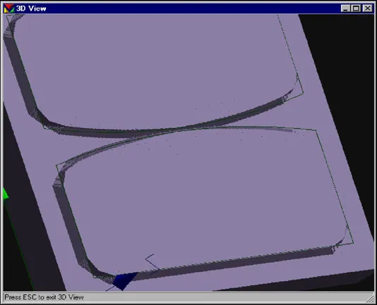
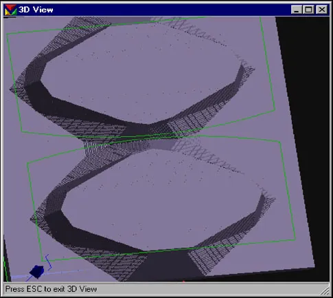
Simulation of a classic bowl and stem etch showing the evolution of the etching profile. Features such as RIE lag, scalloping, feature size dependency can be seen in the simulation.
RECIPE allows you to explore novel structures and allows you to tailor your cross-sections on a PC, rather than performing cumbersome and costly clean room experimentation. For instance, you can easily perform an anisotropic RIE etch, an isotropic etch and a Bosch etch — one right after another! In addition, you can use an isotropic etch to explore front-side release of structures.

Click on the above pictures of validation of RECIPE against experimental results. IntelliSense owes a large debt to its University Partners in the development and validation of RECIPE, in particular, Peking University, Institute of Microelectronics.
RECIPE offers you the ability to simulate a variety of RIE/ICP-related effects. These include:
See how RECIPE and IntelliFAB can help you in process debug
 3D Visualization RECIPE has now been extended to work efficiently in 3D. RECIPE engine can be used within IntelliFAB as well. Composite processing Simulate effects of multiple etches
 Sidewall and etch lag simulation Predict important parameters such as etch lag and sidewall angles Validated simulator Rigorous etch characterization experiments Validated database RSM-derived etch database
 Quick results Faster than performing a real etch
FabViewer supports several commercial process design kits!
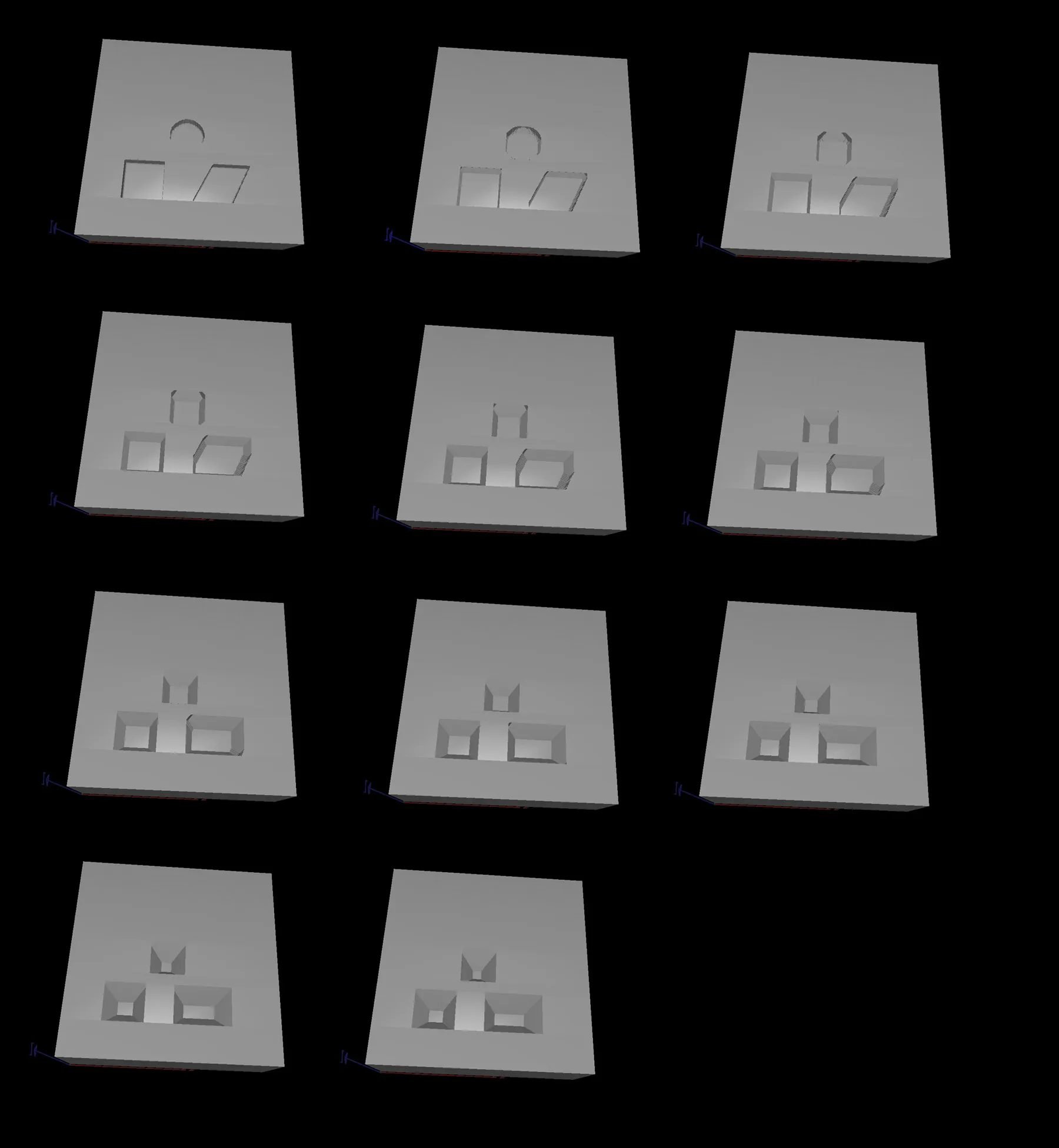
IntelliFab includes FabViewer, an easy-to-use process visualization tool that allows users to quickly visualize a process flow created in IntelliFab. Users can view their structure at each process step or set the simulation to play on a loop. The ability to view cross-sections at any angle or orientation makes it easy to debug the process or perform a failure analysis.
.webp)

With FabViewer, you can see exactly what your MEMS device looks like – before it’s been created!
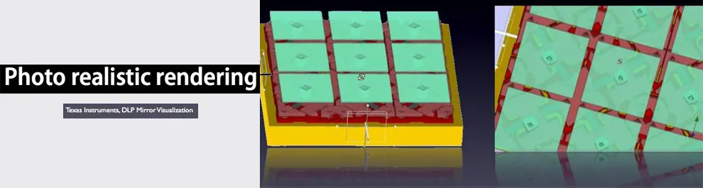
IntelliSense is now providing a free version of FabViewer for use with commercial PDKs. Users can import their own GDSII masks and view photo-realistic renderings of their design using our included PDKs. This FabViewer package comes preloaded with several commercial PDKs including the popular MUMPs from MEMSCAP Inc.
Photo-realistic rendering of MEMS structures makes FabViewer an absolute must-have for engineers creating presentations for a design review or professors making slideshows for a lecture. Seven different resolution settings enable users to adjust the simulation speed and image quality to their liking. Even at the highest resolution, the simulation of highly complex MEMS structures and process flows is completed in minutes.
And with one click you can export the entire process flow to PowerPoint, ideal for documentation or just getting the point across! Download the PPT/PDF file below to take a look at the high-quality export capability.

Electrothermal Actuator (3D):
Use FabSim to quickly create photo-realistic process models and cross-sections using full physical simulation.
FabSim is a visualizer that enables you to view and debug your complex process flow before setting foot in the cleanroom. FabSim works with IntelliFab to render each process step in vivid detail. Users can view their structure at each process step and view cross-sections at any angle for easier debugging.


IntelliSense has long been the MEMS industry leader in physical process simulation with tools like RECIPE for DRIE etch simulation, IntelliEtch for wet etch simulation, and Exposure for lithographic process simulation. All of this functionality is integrated into IntelliSuite’s flagship process simulator, FabSim. The new simulator makes it easy to create photo-realistic process models using full physical simulation, rather than traditional geometrical methods.

FabSim and FabViewer have a very similar look and feel. FabSim can perform all the same functions including deposition, UV lithography, etching, bonding, and so on. It even supports the same useful PowerPoint export ability. The main difference is in the solving method. FabViewer uses basic voxel-based geometry while FabSim uses physical solving methods, yielding more accurate results. The difference is most noticeable when dealing with Si wet anisotropic etch steps. The image below shows an example of wet etching using both tools.
<For both etch types, FabSim uses a CA model for more accuracy and reduced simulation time.
The SU8 lithography module uses a 3D dynamic CA model. The simulation speed is greatly improved compared with a static 3D CA model.
Use Exposure to simulate SU-8 photoresists during exposure, PEB, and development processes.
Exposure is a module that simulates the physical phenomenon and chemical reaction of SU-8 photoresists during the exposure, PEB, and development process which are the focuses of UV lithography modeling.
It includes all steps of UV lithography modeling:
A.Inclined light intensity distribution modeling
B.Exposure modeling
C.PEB modeling
D.Development modeling
Exposure can predict the developed profiles of SU-8 photoresists. Also, it can analyze the intensity distribution impact on the developed profile of SU-8 photoresists.
A series of experiments for inclined/multi-directional UV lithography of SU-8 photoresists have been performed to verify the Exposure module’s accuracy. The following two cases will show the influence of substrate reflection on the oblique structures. SU-8 was coated on both silicon wafers and glass wafers with TiO2 film.
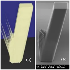
Figure 1. Simulation and experimental results for SU-8 oblique pillar with weak reflection-induced structures on bare silicon wafer. 240 μm thickness SU-8 was exposed at a UV light intensity of 2.6 mW/cm2 for 380 s at 23.5°.

Figure 2. Simulation and experimental results for SU-8 oblique pillar with strong reflection-induced structures due to prolonged exposure time. 140 μm thickness SU-8 was exposed at a UV light intensity of 2.6 mW/cm2 for 600 s at 23.5°.
Case 2. SU-8 structures on TiO2 substrate

Figure 3. Simulation and experimental results for L-shape oblique SU-8 structure with no reflection-induced pattern
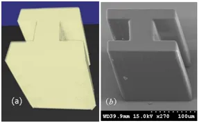
Figure 4. Simulation and experimental results for I-shape oblique SU-8 structure with no reflection-induced pattern
LOCATION
 220 Broadway, Suite 102, Lynnfield, MA 01940, USA
 sales@intellisense.com
 +1781.933.8098
fff
india@intellisense.com +91 98866 35654© IntelliSense. All rights reserved.


