


Unlock the power of multiphysics simulation with IntelliSense's comprehensive suite of multiphysics modules. Our advanced technology enables engineers and scientists to tackle a diverse array of complex challenges across multiple disciplines.
At IntelliSense, we understand the importance of seamless integration and robust capabilities. That's why our multiphysics modules are meticulously designed to offer unparalleled accuracy, efficiency, and versatility. Whether you're working in computational fluid dynamics, electromagnetics, structural mechanics, or heat transfer, our modules provide the tools you need to drive innovation and achieve breakthrough results.
With intuitive interfaces and state-of-the-art algorithms, our modules empower users to explore, analyze, and optimize their designs with ease. From simulating fluid flow dynamics in aerospace applications to modeling electromagnetic phenomena in electronic devices, our solutions deliver precise insights that drive informed decision-making and accelerate product development cycles.
Experience the next level of simulation technology with IntelliSense's multiphysics modules. Explore our offerings today and discover how you can revolutionize your engineering and scientific workflows. Unlock new possibilities, streamline processes, and stay ahead of the competition with IntelliSense.
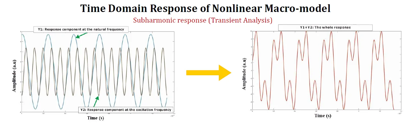
In 1995, we released the first fully coupled thermal,electrostatic and mechanical (TEM) analysis tool for MEMS. Since then, our multiphysics capabilities have grown by leaps and bounds, encompassing all domains of physical phenomenon including fludics, magnetostatics, and high frequency electromagnetics. At the same time, we've added support for orthotropic, anisotropic, piezoresistive, piezoelectric and anisoelastic materials. While the breadth of analyses have grown to include, linear and non-linear, static, steady state, transient, frequency domain and harmonic simulations. A bevy of enhancements now allow you to perform parametric loading, take into account processing conditions, or greatly reduce problems sizes by sub-modeling. You can also use the tool to create macromodels for integration with system modeling tools.


IntelliSuite provides some of the most extensive field coupling in the industry. Users can perform a wide range of coupled simulations ranging from:
Electrothermal
Electromechanical
Thermomechanical
Magnetomechanical
Piezoacoustic
Electromechanical, Electrothermal and Thermomechanical with contact
Thermal-Electrostatic-Mechanical
Thermal-Electrostatic-Mechanical with contact physics
Thermo-Electrostatic-Mechanical with rayleigh damping
Thermo-Electro-Mechanical with full fluid structure interaction (Navier-Stokes)
Electro-Magneto-Mechanical
Piezoresistive-Mechanical
Piezoresistive-Electrothermal
Piezoelectric-Thermal-Mechanical
Piezoelectric-Mechanical-Fluid Structure Interaction
... and much much more

It is little wonder that IntelliSuite is used in corporations ranging from blue-chips to startups and is part of the MEMS curriculum in leading universities worldwide.

IntelliSuite Multiphysics is not a pure Finite Element based tool like Ansys, Comsol or a number of other tools on the market. IntelliSuite uses a mixed formulation that couples Finite Element methods with other numerical computing techniques which are optimized for the fields being computed. For instance, Electrostatic fields or high frequency impedance calculation use a boundary element formulation.
IntelliSuites multiphysics capabilities support 64bit multiprocessor and multicore computing to fully take advantage of modern computing trends.

Boundary Element Method (BEM): Electrostatics, Impedance Extraction
Finite Element Method (FEM): Thermal, Mechanical, FullWave Electromagnetics
Volume of Flow (VoF) and Finite Volume (FV): Fluidics, Electrokinetics, Chemical Reactions
Schwartz-Christoffel Mapping (S-C): 2D Electrostatics (SYNPLE)
Surface Tracking Algorithms : Droplet microfluidics
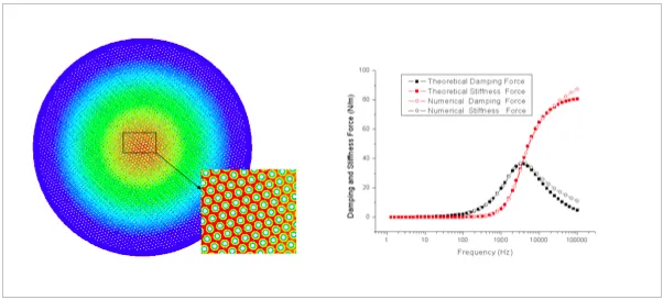
Quick Rayleigh Solver: Fluidic damping
Advanced Precorrection: Precorrected FFT (pFFT++) techniques used to improve convergence
Model Order Reduction: GMRES, Arnoldi techniques are used to reduce problem sizes
Multiprocessor: OpenMP and other multiprocessor solvers are used for quick solution times
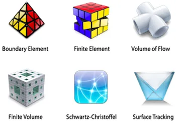
IntelliSuite uses a number of solvers optimized for the computation at hand rather than relying on Finite Element Method as the only tool.
Boundary element techniques use Greens theorem to convert volume integrals into surface integrals, as a result only surface meshes are needed for Electrostatics and Electromagnetic computations. In addition, electrical meshes can be decoupled from mechanical meshes- a big time saver. In many MEMS devices, electrostatic fields are confined to areas of low deformation and high stresses occur in flexures with low electrostatic fields. By optimizing computational meshes for each field, users can simulate large MEMS devices with ease.
In a number of benchmarks, Fastfield solvers are 2-10X faster than pure finite element solvers. Use of surface meshes instead of volume meshes obviates the need for meshing air gaps. In addition, there is no costly remeshing that is required during the deformation of MEMS devices. Fastfield solvers can handle large deformations, contact and post contact problems in coupled field simulations.
IntelliSuite gives you a full range of tools to model heat transfer phenomena. Designing a thermal actuator or a bolometer? Want to calculate thermal stresses during packaging? Want to model Joule heating or heat flux? No problem! This tool does it all. Or use the tool in conjunction with other analysis modules to calculate the temperature coefficient and response of your device.


The electrostatic module of IntelliSuite is designed from the ground up for real world MEMS problems, like a 200 radial comb drive or a corrugated RF-MEMS device. Other CAD tools run into severe limitations while solving real world problems and have to use toy models. Not IntelliSuite! With our innovative Exposed Face Meshing algorithms, you can solve extremely large problems with ease. In fact, you can even investigate second order effects such as levitation due to the ground plane (important in most comb drive structures), temperature coefficient of your capacitors, or charge buildup that can cause potential arcing.
IntelliSense uses a boundary element formulation to capture the electrostatics, this means that users do not have to mesh the electrostatic gaps. A surface mesh is all that is needed! Multi-dielectric problems, dielectric discontinuities, parasitic capacitance can all be modeled accurately without resorting to costly trial and error in the fab.

One of the strong suits of IntelliSuite is its unparalleled mechanical analysis capability. The mechanical module is seamlessly integrated with the thermal and electrostatic modules to perform fully-coupled analyses. IntelliSuite comes with a full-featured mechanical module that can solve the most complex linear or non-linear, transient or steady-state, static or dynamic problems. Stress and strain calculations, modal and buckling analyses, and frequency responses can all be performed with ease. Full squeeze film damping, dynamic response to complex vibration inputs, shock analysis, and Q factor calculations are equally easy to derive. Difficult problems such as the shift of natural frequency due to voltage, stress loading, or the effect of residual processing stresses on device performance are easy to analyse.


IntelliSuite really shines when it comes to contact, post-contact, and micro-assembly analysis. Other MEMS CAD tools are limited to analyzing single dielectric layers with artificial air stops and make you specify contact faces a priori. IntelliSuite avoids such limitations. Our proprietary algorithms take into account multi-dielectric moving or deformable boundaries and help you locate the exact point of contact. IntelliSuites contact analysis goes way beyond the reduced-order models and other gross simplifications and can help you model complex post-contact phenomena such as hysteresis.
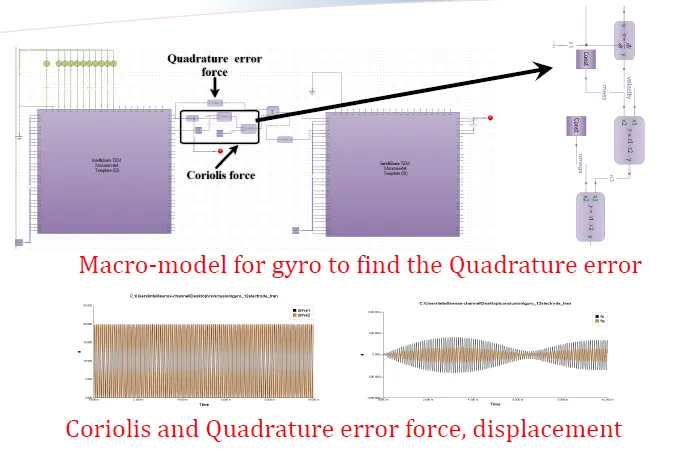
The TEM Module is fully coupled with IntelliSuite’s PiezoMEMS module, the most sophisticated piezoelectric and piezoresistive modeling tool in the industry. Considering piezo actuation for your MEMS device? You can investigate the voltage dependency of the natural frequency, calculate the Q factors in different packaging environments, or apply time-varying loads with ease. You can also look at a floating conductor voltage as a function of time-varying loading, an important factor in acoustic transducer and microphone design.


IntelliSuite is the only tool on the market to offer fully-coupled linear and non-linear thermal-electrostatic-electromagnetic-mechanical simulations. TEM coupled with the ElectroMagnetic module can be used to simulate static and frequency responses of magnetic or electromagnetically actuated MEMS devices. Lorentz force-driven actuators such as scanning mirrors, switches, and mechanisms can be simulated wth ease.

IntelliSuite also includes the worlds first NEMS simulator, allowing you to simulate nano-scale structures in conjunction with micro-scale features. The NEMS module can be used to perform thermo-electro-mechanical simulations on a nano-scale. Among other applications, the NEMS module can be used for simulating nano-scale resonators, CNT-based sensors, and carbon nanowires (CNWs).
This is particularly useful in simulating the emerging class of carbon nanotube (CNT) based sensors which combine micro-scale structures with nano-scale CNTs. Users can perform piezoresistive and electro-thermal-stress simulations to understand the CNT response to thermoelectromechanical loading.
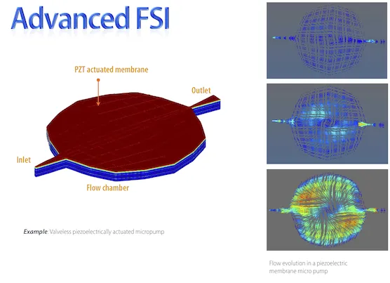
IntelliSuite now features full Fluid-Structure Interaction capabilities. FSI simulations can be performed in time or frequency domain (important for extracting fluidic damping in MEMS). The picture above shows the evolution of flow patterns in a valveless piezoelectrically actuated pump.
TEM is also fully coupled with IntelliSuite’s Microfluidic module. With the capability to analyze advanced fluid-structure interaction, IntelliSuite makes it easier than ever to model complex devices like piezoelectrically-actuated micropumps, fluidic damping in large micromirror arrays, and micromechanical valves.

Linear and non-linear analysis
Static, steady-state, and transient analysis
Fully 3D coupled dynamics analysis
Parametric variations
Support for orthotropic and anisotropic materials
Takes into account fabrication process-induced effects
Sub-modeling, symmetry, and other size-reducing techniques
Animation and color mapping of results
Export and import to/from other engineering CAD tools
Electrostatic pressure, potential and charge distribution
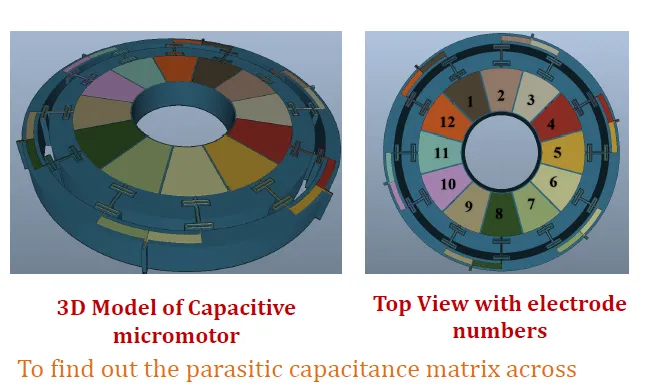
Capacitance matrix derivation
Parasitic calculations
Boundary Element based electrostatics
No need for meshing electrostatic gaps
Stress-displacement calculations (principal and invariant stress calculations)
Natural frequency and modal analysis
Dynamic analysis with external force/acceleration loading
Shock analysis
Q factor calculation
Damping analysis (including squeeze film effects)
Definition of customized functions for external loading, up to 500 points in defining the curve
Small and large displacement theory
Residual stress incorporation
Multiple simultaneous input loading
Contact and post-contact analysis
Hysteresis analysis
Microassembly and latching modeling
Popup and bistable elements
Full die- and board-level packaging modeling
Thermo-mechanical analysis
Effect of packaging in low pressure environment
Incorporation of epoxies, dams, filler and getter materials
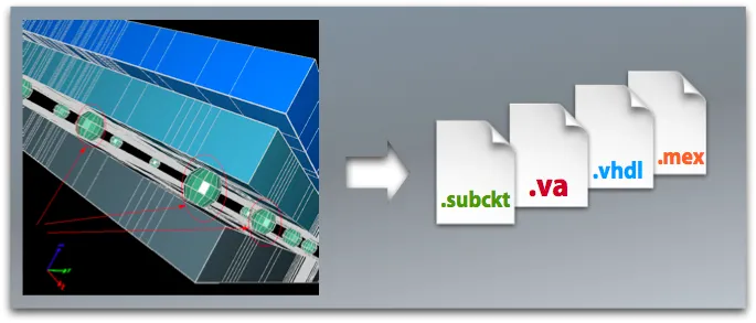
Macromodel derivation of input to SPICE and related tools
Advanced high-frequency analysis and SPICE model generation
Heat transfer problems
Conduction or convection modeling
Joule/resistive heating modeling
Temperature distribution and gradients
Exposed face meshing to decouple mechanical and electrostatic meshes
Boundary Element based Electrostatics
Displacement due to voltage and thermal loading
Capacitance due to voltage and thermal deformation
Natural frequency shift due to voltage or temperature loading
Pull-in voltage, contact and hysteresis loop calculations
Full multi-dielectric capabilities
Stress, temperature, potential, charge, and pressure distribution
Joule/resistive heating actuation
Assembly and latching analysis
Post-assembly coupled analysis
Natural frequency and mode shapes as a function of loading
Heat transfer: radiation, conduction, and convection
Squeeze film damping
Fluid-structure interaction
Piezoresistive and piezoelectric modeling
Displacement and deformation due to voltage loading
Natural frequency and mode shapes as a function of loading
Analyze, simulate, and design piezoelectric transducers, sensors, and actuators
Static analysis (stresses, strains, voltages, etc)
Frequency shift due to loading and frequency sweep analysis
Mode-based transient analysis
Direct integration transient analysis (both auto- and fixed-increment analyses)
Time-dependent loading
Floating conductor voltage determination

As a packaging engineer, IntelliSense offers you tools for thermal, mechanical and high-frequency modeling of your devices. Parametric scripting capabilities allow you to effortlessly create a range of packages, such as SOICs, DIPs, QFPs etc. What's more, wafer-level encapsulation and related stress analyses may be performed with ease. As a result, you can wrap up your projects quickly and efficiently!

Working together, IntelliSuite and SYNPLE give test engineers a straightforward method for creating parametric test structures and design of experiments (DoE) during the layout process. What's more, our analysis and system simulation tools allow you to perform a vast subset of MIL-STD (750/883), JEDEC (JESD22) and Telcordia (Belcore) tests in software before the actual fabrication. For success in your next test, turn to IntelliSuite!
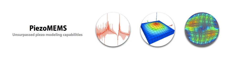
IntelliSuite ships with the most sophisticated piezoelectric and piezoresistive modeling capabilities in the industry. Our PiezoMEMS module represents a complete solution for MEMS designers considering piezo-sensing or piezo-actuation mechanisms.

If you are designing piezo-based sensors and transducers, or investigating piezo-acoustic coupling, you will find our design tools invaluable and unsurpassed. Considering piezo actuation for your MEMS device? IntelliSuite can handle your needs such as time varying loading, floating conductors, full thermo-electromechanical modeling and high frequency analysis.
Our piezo capabilities are designed for real world applications such as film bulk acoustic resonators (FBAR), surface acoustic wave (SAW) devices, Quartz Crystal Gyros,Piezoelectric pumps, Energy Scavengers and piezoresistive sensors such as manifold air pressure (MAP) sensors.
Our integrated thermoelectromechanical modeling of piezo-materials allows you to perform static, transient, direct-integration or mode-based analysis for linear or non-linear problems. You can investigate the voltage dependency of the natural frequency, calculate the Q factors in different packaging environment, or apply time varying loads with ease. In addition, you can look at a floating conductor voltage as a function of time varying loading which is important for acoustic transducer and microphone design. PiezoMEMS now supports fully integrated piezoelectric and fluid structure interaction (FSI) modeling.
IntelliSuite can perform full high frequency analysis for a piezoelectric material under cyclic loading allowing you to calculate both series and parallel resonances. In addition, Y-, Z- and S-parameters, reactive charge density and charge can be extracted with ease.

PiezoMEMS now features multiprocessor enabled solver for FBAR/SAW type devices. Users can perform time domain or frequency domain analyses to understand the behavior of their devices. Impedance of the devices can be exported as a Touchstone file that can be used in other circuit simulators.
IntelliSuite also features a fast piezo impedance extraction algorithms that can be used to quickly simulate the frequency response of the device and the phase noise.
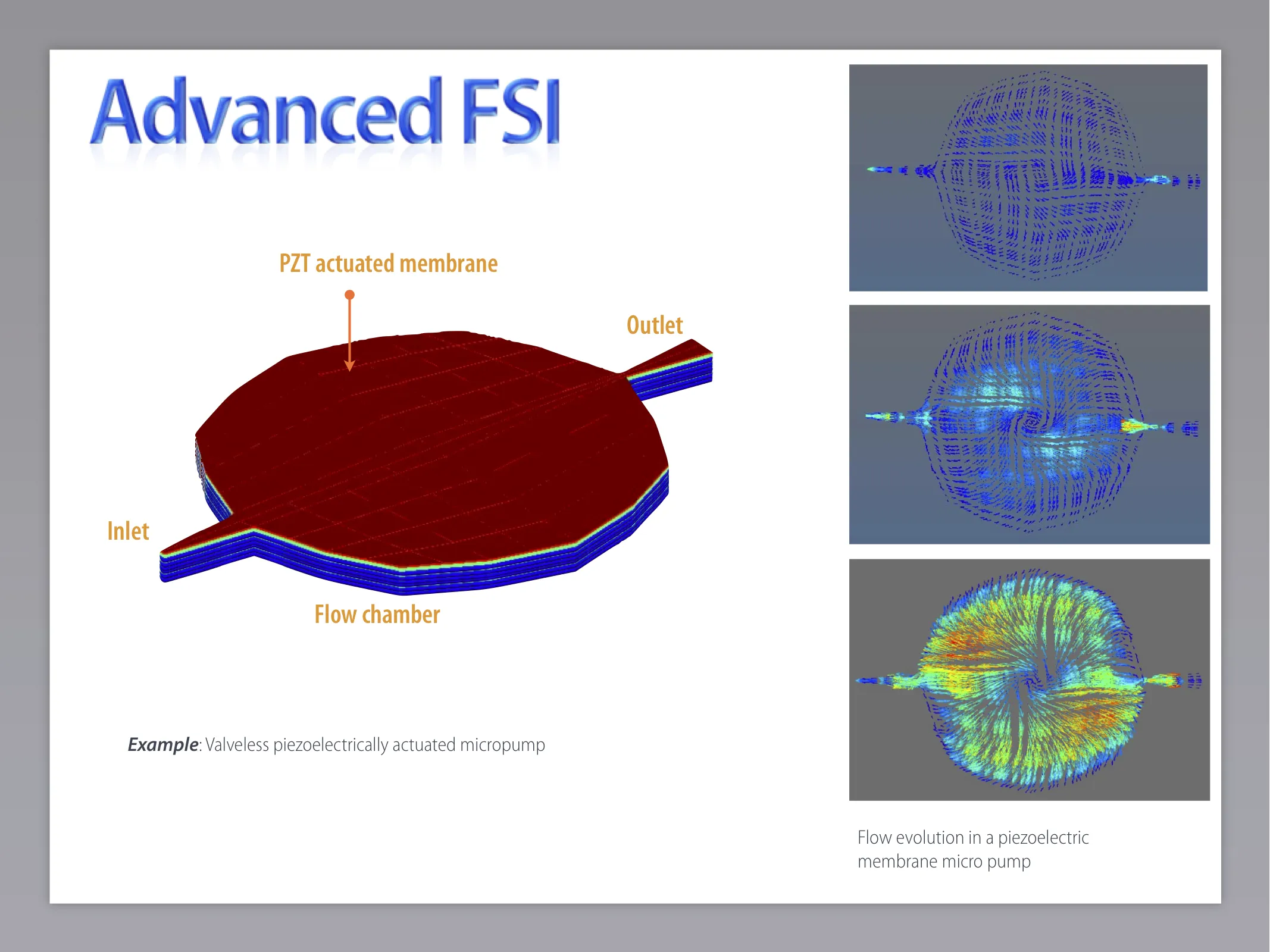
Advanced fluid structure capability allows you to model and optimize complex piezo-drive pumps. Flow rates, nozzle dimensions can be optimized with ease.
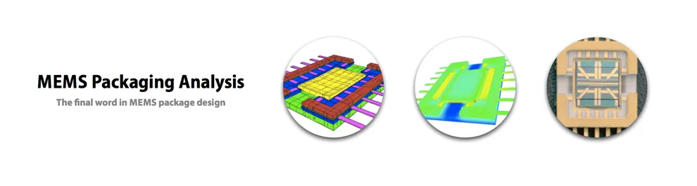
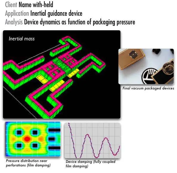
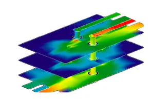
One of our dictums is to concurrently design MEMS devices and packaging. Far too many MEMS projects fail due to a lack of packaging considerations upfront. IntelliSuite simplifies the packaging of MEMS devices, reducing the cost of packaging development. The tools you need to perform die level and board level packaging analyses come standard with IntelliSuite. Packaging related stresses, CTE mismatches, shock effects, effects of packaging pressure on device damping, parasitic effects and high frequency electromagnetic effects can all be modeled with ease.

Learn how IntelliSuite can help you in Packaging analysis. From device level to package level, from thermo-mechanical to high frequency modeling. There is a solution that is right for you
(Click to expand)
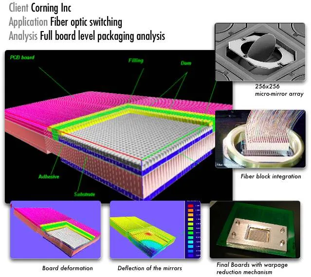


IntelliSuite solves most complex packaging problems involving linear and non-linear, static, frequency, and dynamic behavior. Stress, strain and warpage calculations, modal and buckling analysis, and the thermal-electrical (joule heating) response of packaged devices can all be performed with ease.
Users can model the dynamic response of packaged devices to complex vibration inputs, perform shock analysis, incorporate convective heat losses, and calculate Q factors. Fully coupled squeeze film damping modeling allows you to determine device performance as a function of package pressure. This allows you to perform JEDEC, MIL STD, or Belcore tests on packaged devices before costly device fabrication.

MEMS-ASIC integration modeling
Print Quality:
 PDF
PDF
As MEMS make their successful entry into mobile devices, the demand for slim profile packages becomes paramount. MEMS devices have started to leverage IC stacking technologies such as wafer bumping, die-on-wafer assembly, through-silicon vias (TSV) and towards low-cost Wafer Level Chip Scale Packages (WLCSP). As the MEMS subsumes the package into the structure, the need for efficient package modeling and compensation of packaging effects at the die level become important.
One of the most innovative features is the ability to include packaging effects on the device performance into the system models. Package extraction and sub-modeling techniques allow you to estimate the impact of the package stresses and temperature effects on the device performance.
(Click to enlarge)

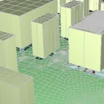
IntelliSuite allows you to go from your board layout [DXF, GDS, or Gerber] to a high fidelity 3d hex meshed model that is ready for analysis in click of a button.
Advanced meshing tools allow you to create complex meshed models from your board DXF layout in a click. You can use 3DBuilder or our new Hexpresso mesher to automate your modeling and mesh creation process.
Import your DXF layout, set the layer elevation and thickness and tag the purpose of each layer (via, strucutural, metal, conformal coating etc.) and we take care of the rest! High fidelity hexahedral meshes are created automatically, saving you time and effort.
Packaging analysis can now capture fluidic damping and spring force for complex MEMS structures. Our macromodel techniques now extend to fully capture fludic dissipation and automatically include ambient damping into system simulations. Fluidic damping can be captured for each of the modes of interest.
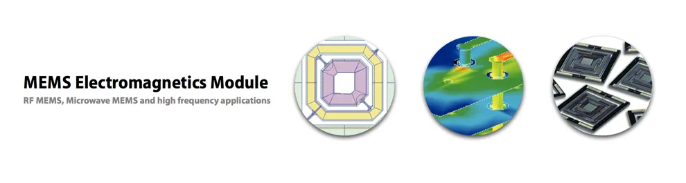
For high frequency RF MEMS and Microwave MEMS devices such as RF switches, filters, and inductors, users can model package related artifacts such as EM coupling between traces, parasitic or substrate coupling, crosstalk, package and board resonance artifacts, impedance mismatches, and reflection noise. Full circuit-package interaction studies and S-, Z-, and Y-parameters can also be derived.

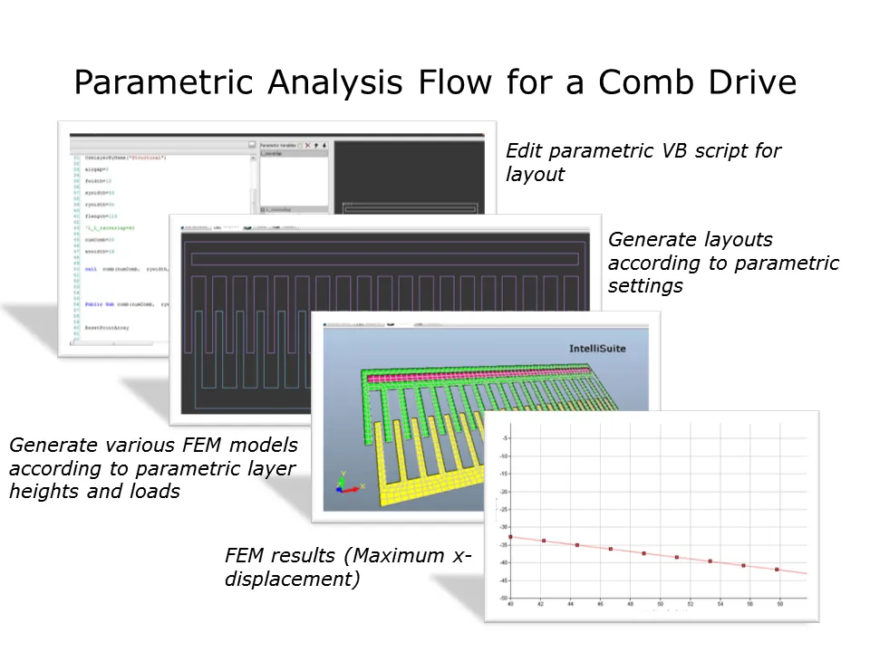
Advanced parametric analysis is simpler than ever before with Parametric Designer. This customized parametric analysis tool uses VBScript as an input to automatically generates masks, 3D models and meshes. After applying boundary conditions and loads on a single model, Parametric Designer begins an unattended multiphysics-based parametric analysis, yielding a detailed report in the end.
LOCATION
 220 Broadway, Suite 102, Lynnfield, MA 01940, USA
 sales@intellisense.com
 +1781.933.8098
fff
india@intellisense.com +91 98866 35654© IntelliSense. All rights reserved.